
Exploring Unique Nanophotonic Phenomena by Electron Beam
To address ever-increasing volume of information and communications, there is an urgent need to develop photonics-electronics integrated devices for faster optical communications and information processing with less power loss. New developments in optical control using nanostructures are required because confining light to nanospace not only reduces the size of devices but also enhances the light-matter interaction, leading to the realization of high-speed, highly efficient devices.
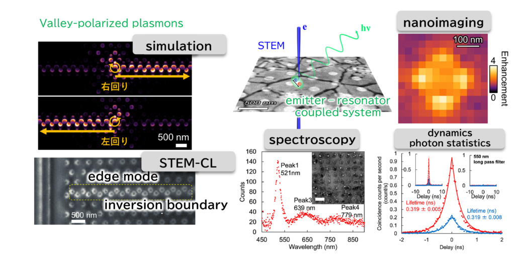
Using electron energy loss spectroscopy (EELS), which is equivalent to absorption spectroscopy, and cathodoluminescence (CL), which analyzes the emission, we are searching for novel surface plasmon modes in nanostructures, and deepen understanding emitter-resonator coupled systems at the nanoscale.
Recent microfabrication techniques allow us to design and fabricate artificial crystals with periodic arrays of nanostructures, and to control plasmon propagation based on band theory. For example, properties derived from the geometry of crystal structures, such as topological insulators and valley polarization, are concepts that can be applied to various waves, including photons and plasmons. We aim to create new degrees of freedom to create new functional devices in combination with nanomaterial systems.
References
Cathodoluminescence Saturation Imaging to Visualize Emitter–Resonator Coupling
Hikaru Saito, Yuuichiro Kimura, Kentaro Matsuzaki, Yoshikazu Adachi, Sotatsu Yanagimoto, Kosuke Watanabe, Miki Inada, Takumi Sannomiya
ACS Nano 2025, 19, 21, 19590–19598
Light Emission Enhancement on Nanostructured Surfaces Quantitatively Evaluated by Cathodoluminescence Coincidence Counting
Tomoyasu Fujimaru, Hiromu Tanaka, Masato Inamata, Midori Ikeuchi, Hidehiro Yamashita, Hiroya Miyazaki, Takashi Gondo, Satoshi Hata, Mitsuhiro Murayama, Hikaru Saito
ACS Photonics 2025, 12, 6, 3073–3081
Valley-polarized plasmonic edge mode visualized in the near-infrared spectral range
Hikaru Saito, Daichi Yoshimoto, Yuto Moritake, Taeko Matsukata, Naoki Yamamoto, Takumi Sannomiya
Nano Lett. 2021, 21, 15, 6556–6562
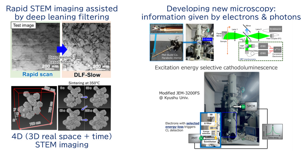
Development of Electron Microscopy Combined with Information Science and Optical Measurements
Analysis of nanostructures and local chemical compositions using electron microscopes is indispensable in various fields of material and biological science. In particular, “in situ observation” is becoming increasingly important because it directly reveals how nanostructures and functions change in response to external stimuli such as heat, electric field and magnetic field.
The key to in-situ observation is high-speed imaging. We have previously developed high-speed scanning transmission electron microscopy (STEM) imaging utilizing deep-learning-based noise filtering. This method has successfully reduced the data acquisition time for 3D observation (tomography) of thick samples, from several tens of minutes to just five seconds. In combination with special specimen holders (developed by Mel-Build co.), we have also achieved video-rate STEM imaging of material heat treatment and nanoscale four-dimensional (three-dimensional space + heat treatment time) measurement of powder sintering. Such four-dimensional nano-measurements are applied to high-precision parameter estimation in conjunction with computational science, suggesting a new materials development platform utilizing digital twins.
The development of these advanced electron microscopy methods has been applied not only to nano-optics (our main specialty), but also to various materials fields such as catalysts, thermoelectric materials, superconducting materials, and battery materials, as well as to geological analysis of the asteroid Ryugu for the Hayabusa 2 project (JAXA).
Furthermore, in optical measurement, we began development of an “excitation event selective cathodoluminescence microscope” in 2023. This microscope measures the correlation between inelastically scattered electrons and photons emitted from the sample on an event-by-event basis, revealing several elementary processes from the excitation to light emission.
References
Five-second STEM dislocation tomography for 300 nm thick specimen assisted by deep-learning-based noise filtering
Yifang Zhao, Suguru Koike, Rikuto Nakama, Shiro Ihara, Masatoshi Mitsuhara, Mitsuhiro Murayama, Satoshi Hata, Hikaru Saito
Scientific Reports volume 11, Article number: 20720 (2021)
Deep learning-based noise filtering toward millisecond order imaging by using scanning transmission electron microscopy
Shiro Ihara, Hikaru Saito, Mizumo Yoshinaga, Lavakumar Avala, Mitsuhiro Murayama
Scientific Reports volume 12, Article number: 13462 (2022)
In situ electron tomography for the thermally activated solid reaction of anaerobic nanoparticles
Shiro Ihara, Mizumo Yoshinaga, Hiroya Miyazaki, Kota Wada, Satoshi Hata, Hikaru Saito, Mitsuhiro Murayama
Nanoscale, 2023, 15, 10133-10140
High-fidelity phase-field simulation of solid-state sintering enabled by Bayesian data assimilation using in situ electron tomography data
Akimitsu Ishii, Akinori Yamanaka, Mizumo Yoshinaga, Shunsuke Sato, Midori Ikeuchi, Hikaru Saito, Satoshi Hata, Akiyasu Yamamoto
Acta Materialia Volume 278, 1 October 2024, 120251
A dehydrated space-weathered skin cloaking the hydrated interior of Ryugu
Takaaki Noguchi, Toru Matsumoto, Akira Miyake, Yohei Igami, Mitsutaka Haruta, Hikaru Saito et al.,
Nature Astronomy volume 7, pages170–181 (2023)
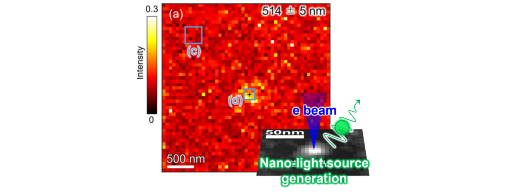
Precisely Positioned Generation of Perovskite Nano-Light Sources by Electron Beam Irradiation
Nano-integrated optical systems composed of nano-light sources (e.g. quantum dots) and nanophotonic components such as nanocavities and waveguides potentially achieve unprecedented physical properties that cannot be achieved by individual materials or structures alone. To maximize this synergy, new process methods that can precisely control their relative positions are required. We have recently discovered a phenomenon that generates perovskite nano-light sources at desired locations with nanometer accuracy by electron beam irradiation. It is known that some perovskite nanoparticles can function as single-photon sources at room temperature, when their sizes are smaller than the exciton Bohr radius. We are experimentally exploring how to control the structure and properties of the generated nano-sources to realize single-photon source arrays applicable to quantum devices.
References
Nano-light source generation by electron beam irradiation of CsPbBr3/Cs4PbBr6 composites
Hikaru Saito, Kotaro Kihara, Midori Ikeuchi, Sotatsu Yanagimoto, Tetsuya Kubota, Keiichirou Akiba, Takumi Sannomiya
Appl. Phys. Lett. 127, 261102 (2025)