

About Saito Laboraory
“Nanofabrication that is possible only with an electron microscope”
Our group is a relatively new field within IMCE, having started in 2025. In order to promote the Institute’s overall goal of “establishing a practical platform for creation of advanced materials with precisely designed nanostructures and characterization of their properties and functions,” we are conducting research and development of both hardware and software for electron microscopes that can directly measure structures and electronic states at the atomic level, with the aim of leading to the discovery of new materials and functions and the creation of new devices.
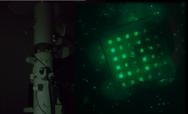
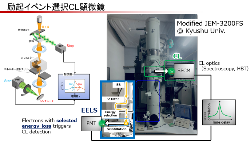
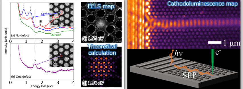
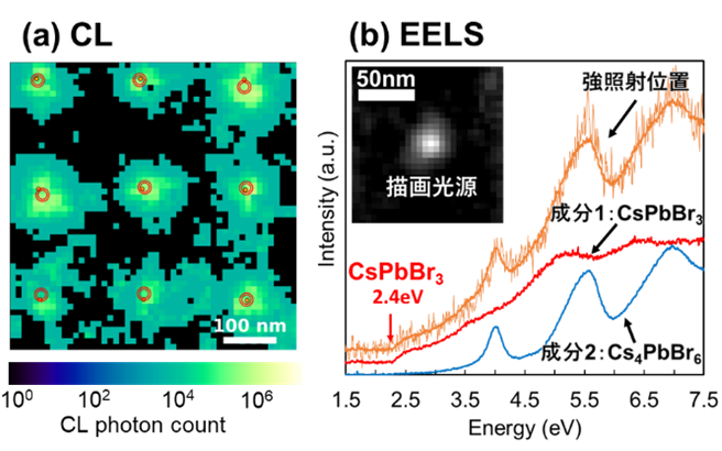
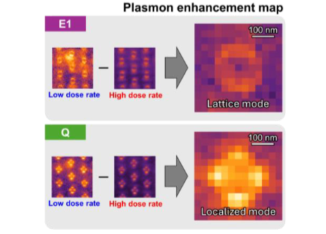
We focus on electron microscopy techniques, such as electron energy-loss spectroscopy (EELS) and cathodoluminescence (CL), which allow direct access to electronic states and optical functions. We are working to pioneer new optical measurements that utilize the nature of both electrons and photons, and to further advance them by incorporating information science techniques such as machine learning. By utilizing these uniquely developed measurement techniques, we are promoting research such as nanophotonics, topology-based optical waveguiding, and exploring new phenomena that emerge in integrated devices of nano-optical elements and functional materials.
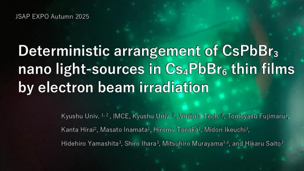
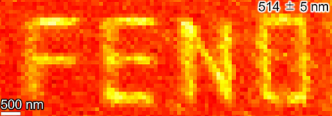
Electron beams are also a direct manufacturing tool for processing materials at the nano level (e.g. electron beam lithography). We are pioneering nanofabrication that can only be realized by real-time monitoring with an electron microscope, such as nano-light source drawing using electron beams. By bringing together various knowledge from condensed matter physics, material chemistry, materials science, process engineering, etc., we will discover and develop the nano-processes that will serve as the seeds for next-generation optical devices utilizing the quantum nature of photons.